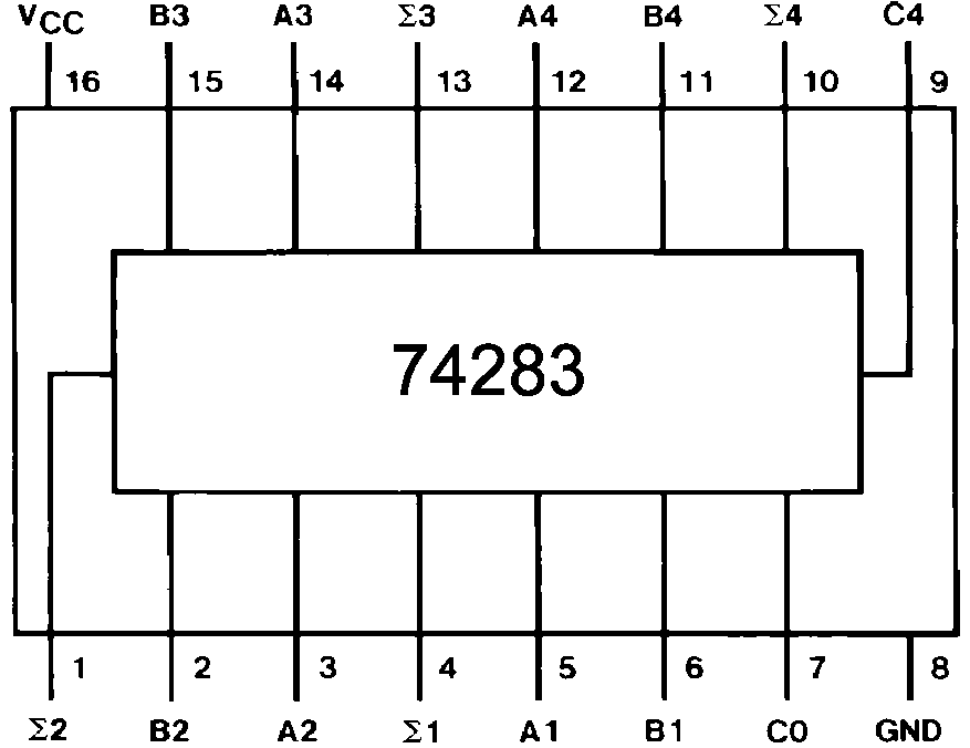
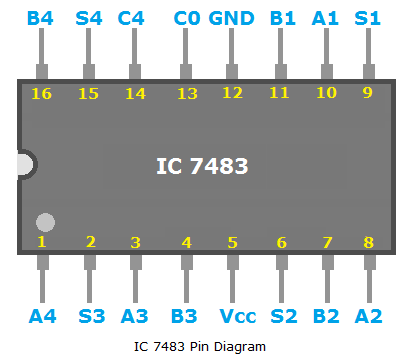
Pin Diagram Of 7483 Ic
Design a 1 digit bcd adder using ic 7483 and explain the operation for Truth 7483 etechnog Circuit diagram for 4 bit binary adder using ic 7483 » wiring core
Design a 1 digit BCD adder using IC 7483 and explain the operation for
Diagram integrated functions configuration connection circuits elektropage Manpreet singh (m$k) Design and explain 8 bit binary adder using ic 7483.
Circuit diagram for 4 bit binary adder using ic 7483
Gate xor ic circuit 7483 table exclusive diagram logic truth 7486 subtraction gates used shown below performing digital electronicsPart 3. parallel adder 3-1) consider an ic 7483, 7483 ic 4-bit binary full adder with fast carryIc 7483 pin diagram, truth table, applications.
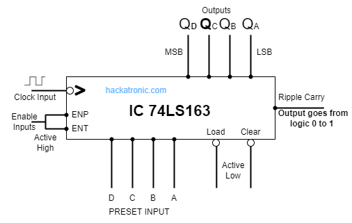
Ic adder bit 7483 using parallel binary pooja joshi description7483 ic adder using bcd Using ic 7485 design an 8 bit comparatorIc74163 pin diagram, truth table & counter circuit » counter ics.

Solved the diagram and results table for the 7483 adder is
Truth applications etechnog7485 comparator digital chip adder circuits students school part high chips outs figure Bcd adder using ic 7483Circuit diagram for 4 bit binary adder using ic 7483.
Adder bcd 7483 ic using digit circuit outputDesign and explain 8 bit binary adder using ic 7483. 15 full adder pin diagramGambar 7.3.1. rangkaian aplikasi penggunaan ic 7483.
7483 rangkaian penggunaan
Design and implementation of 10’s complement circuit using ic-7483Design and implementation of a bcd adder circuit using ic-7483 Design and implementation of 10’s complement circuit using ic-7483Pin diagram of 7483 ic.
Circuit diagram for 4 bit binary adder using ic 7483Ic pin diagram & wiring diagram Circuit diagram for 4 bit binary adder using ic 7483☑ functions of integrated circuits.
Adder bit ic 7483 using binary parallel adders four explain ques10 ahead
7483 adder ttl parallel acura radio[diagram] logic diagram of ic 7483 Pin on electronicsLogic diagram of ic 7483. draw a neat circuit of bcd adder using ic 7483 and explain. design a 1.
Four bit adder or subtractor using 7483Digital circuits for high school students (part 2) Circuit diagram for 4 bit binary adder using ic 7483 » wiring corePin diagram of ic 74190 datasheet & application notes.

Ic 7483 pin diagram, truth table, applications
Circuit diagram for 4 bit binary adder using ic 7483 .
.


Using IC 7485 design an 8 bit comparator
15 Full Adder Pin Diagram | Robhosking Diagram

Design a 1 digit BCD adder using IC 7483 and explain the operation for

Circuit Diagram For 4 Bit Binary Adder Using Ic 7483 - Schema Digital

7483 IC 4-Bit Binary FULL ADDER With Fast Carry | Makers Electronics

(Solved) - The 4 bit adder/subtractor circuit implemented with IC 7483 is... (1 Answer

Design and Implementation of 10’s Complement Circuit Using IC-7483